TeamGroup A440 PRO Special 5eries 4TB NVMe review Specifications & Features
TeamGroup A440 PRO Special 5eries 4TB NVMe review Specifications & Features
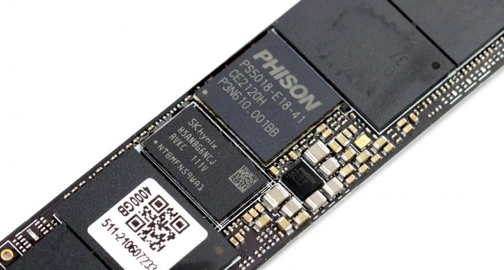
Team as stated is offering four versions of the SSD; 1TB, 2TB, and 4TB, unfortunately not an 8TB model. For endurance, our tested 2TB model has been rated at 1400 TBW. The series will be fitted with TLC written 3D NAND flash memory (vertically stacked over 176 layers). This allows the company to offer proper storage volumes. So instead of using Planar NAND, 3D NAND is used. 3D TLC NAND is physical vertical NAND cell stacking not to be confused with chip stacking in a multi-chip package. In 3D NAND, NAND layers, not chips, are stacked in a single IC. The good news is continued cost reduction, smaller die sizes and more capacity per NAND chip. Also, installed NAND toolsets in the wafer fabs can, for the most part, be reused, thereby extending the useful life of fab equipment. Unleashed by the PCIe 4.0 ready AMD B550/X570 chipset and Intel Rocket Lake-S / Alder Lake-S / Z590/ Z690, the SSD reaches up to an advertised ~7000 MB/sec sequential read – fourteen times the performance of many SATA SSDs and seventy times faster than some hard disk drives. The performance stems from the hugely increased bandwidth of PCIe 4.0 (PCI-Express Generation 4), a feature that will be made available to customers for the first time as part of the AMD X570 chipset and 3rd Generation AMD Ryzen Desktop Processors. Easily fitting into a PCIe 4.0 x4 M.2 slot, the NVMe interface has been bumped upwards to the new 1.4 protocol and high-density TLC NAND combine with a Phison PS5018-E18 controller to enable a new level of single-drive SSD performance. Boasting staggering numbers.
Phison PS5018-E18 controller
Phison, based in Taiwan, is well-known for its flash NAND controllers, which have gained significant traction in recent years. In addition to being built on a Cortex-R5-based processor design, the PS5018-E18 controller is also constructed on TSMC’s 12nm process technology. Furthermore, the controller includes three Cortex R5 cores running at 1GHz, as well as two Dual CoXProcessor 2.0 cores running at a lower clock speed that handle the host’s requests as well as the SSDs’ own NAND management algorithms. In addition, the controller supports the APST, ASPM, and the L1.2 standby power state for efficiency, as well as thermal throttling to guarantee that the system operates at a cool temperature. The MP600, like the Sabrent Rocket 4 Plus, does, however, have a low throttle temperature restriction, similar to the Sabrent Rocket 4 Plus. Thermal throttling is activated when the temperature rises above 68 degrees Fahrenheit. This approach dynamically reduces speed by approximately 50 MBps for every 1 degree Celsius above the temperature limit set by the manufacturer. By upgrading this controller to NVMe revision 1.4, the transfer rate per channel has increased from 800MT/s to 1200MT/s. And when you do the arithmetic, you’ll find that the maximum transfer speed for both sequential reads and writes is approximately 7GB/s. In addition, random read/write performance would be quoted at 1 million IOPS, and all of this would be accomplished with a projected peak energy usage of 3W just for the controller.
NVMe is also known as Non-Volatile Memory Express or the Non-Volatile Memory Host Controller Interface Specification. The idea behind NVMe is to improve the storage stack by optimizing the way an application accesses a Flash device. NVMe cuts corners by removing components within the I/O path like that good old-fashioned RAID controller. NVMe leverages PCIe as transport media which offers high bandwidth and a direct path to the host’s CPU and memory. This, in turn, removes another potential bottleneck, the limited bandwidth of SAS or the latest SATA3 connection. NVMe makes use of your PCI-Express lanes, and as you know… the latest gen 3 PCIe lanes are fast, and thus lift the bottleneck that SATA3 has. Moving from PCIe Gen 2 to Gen 3 doubles the bandwidth available to the add-on cards installed, from 500 MB/s per lane to 1 GB/s per lane. PCIe 4.0 once again doubles that up, Obviously, the hardware you use needs to be Gen 4.0 compatible.
So that the NVMe M.2 units use whatever they are assigned; most motherboards and units now can connect on an x4 link, so that Gen 4.0 x4 link of yours can handle a total bandwidth of 16 GB/s (bi-directional) in PCIe Gen 4.0 mode, whereas the old Gen 1.0 x16 slot would be capable of 2GB/sec (bi-directional). That bandwidth combined with fast NAND and a top-notch controller can allow for massive storage speeds. To be able to make use of the new NVMe based devices inside your PC you have to have a proper driver installed, this can be downloaded at the Samsung website. This enables NVMe devices to function within the existing operating system I/O stack protocol.
SATA 3 (6Gbps)
SATA 6G (SATA 3), the latest revision of your SATA storage unit connectors, will increase the bandwidth on the SATA controller from 3 Gbit/sec to 6 Gbit/s. For a regular HDD that is not really very important. But with the tremendous rise of fast SSD drives this really is a large plus. Typically we get 3000 Mbit/s : 8 = 375 MB/s bandwidth minus overhead, tolerances, error-correction and random occurrences. SATA 3 doubles it up, as such we get 6000 Mbit/s : 8 = 750 MB/s (again deduct overhead, tolerances, error-correction and random occurrences) of available bandwidth for your storage devices. As you can understand, with SSDs getting faster and faster that’s just a much warmed and welcomed increase of bandwidth. Put Sata3 in RAID and you’ll have even more wicked performance at hand. Most motherboards offer only two ports per controller though, so you are (for now) limited to RAID 0 and RAID 1 (stripe or mirror).
What is NAND?
Flash memory is an electronic non-volatile computer storage medium that can be electrically erased and reprogrammed. Introduced by Toshiba in 1984, flash memory was developed from EEPROM (electrically erasable programmable read-only memory). There are two main types of flash memory, which are named after the NAND and NOR logic gates. The NAND type is primarily used in main memory, memory cards, USB flash drives, solid-state drives (those produced in 2009 or later), and similar products, for general storage and transfer of data.
NAND Types
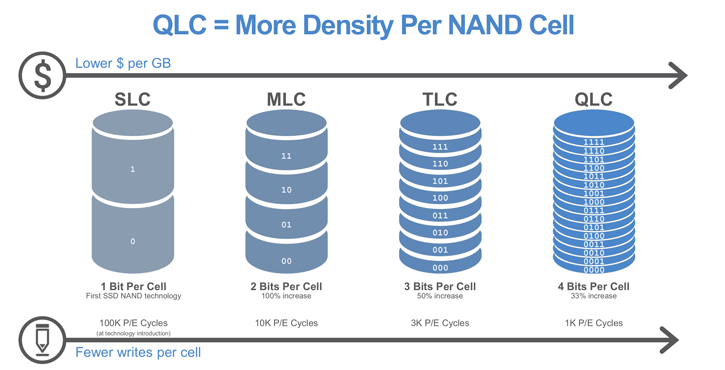
At the beginning, memory cells stored just a single bit of information. However, the charge on the floating gate can be controlled with some level of precision, allowing the storage of more information than just 0 and 1. So you can store more with the same cell? That’s easy cost reduction. Based on such an assumption the (Multi-Level Cell) memory came into play. To distinguish them, the old memory type was called SLC – Single Level Cell. In the year 2019 we now differentiate four primary NAND storage wite methods:
SLC (1 bit per cell written) – fastest, highest cost, best endurance
MLC (2 bits per cell written)
TLC (3 bits per cell written)
QLC (4 bits per cell written) – slowest, least cost, lowest endurance
The decision of choosing between SLC, TLC, QLC and MLC is driven by many factors such as memory performance, number of target erase/program cycles and level of data reliability. The MLC memory endurance is significantly lower (around 10,000 erase/program cycles) compared to SLC endurance (around 100,000 erase/program cycles).
Toggle-mode MLC – Toggle-mode MLC is asynchronous NAND that is supposed to provide similar performance as synchronous NAND, but at a lower price. Independent testing has not verified these claims yet. Toggle-mode MLC is also known as double-data-rate asynchronous NAND. Synchronous and asynchronous NAND, based on spec sheets, look remarkably similar in performance. However, they aren’t. Synchronous NAND is more expensive than asynchronous. Sync NAND is used when performance is everything, such as with gaming systems.
TLC flash memory (triple-level cell flash) is a type of solid-state NAND flash memory that stores three bits of data per cell of flash media. TLC flash is less expensive than single-level cell (SLC) and multi-level cell (MLC) solid-state flash memory, which makes it appealing for consumer devices that use solid-state storage. The drawbacks to using TLC flash are performance, reliability, and longevity. TLC flash has lower write endurance than both SLC and MLC flash. Generally, the more bits of data the cell has, the fewer write cycles it will support. SLC memory cells can withstand up to 100,000 write cycles before failing. A 2-bit MLC memory cell can typically withstand up to 10,000 write cycles before failing. A TLC memory cell can sustain about 1,000 write cycles before failing, which is why thus far it has been limited to consumer-grade applications.