MSI Spatium M450 1TB NVMe SSD review Introduction
MSI Spatium M450 1TB NVMe SSD review Introduction
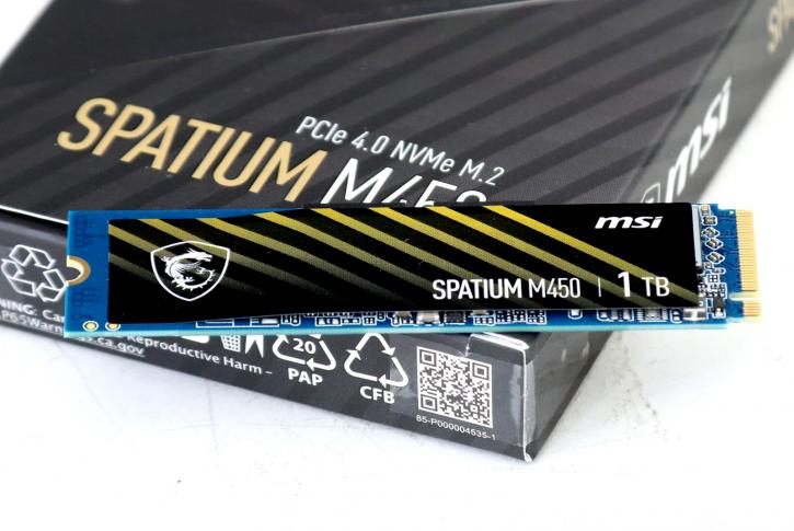
The Spatium M450 is a new M.2 PCIe 4.0 NVMe SSD from MSI. It should be compatible with a wide range of PCs because it was designed first and foremost as a mainstream solution. MSI claims 3600MB/sec sequential read and writes throughput using Phison’s new E19T controller combined with PCIe Gen 4 x4 interface compatibility. Performance varies, as is common, depending on the capacity chosen and whether the host computer supports PCIe 4.0. The storage sizes are 250GB, 500GB, and 1TB, with read speeds of 3500MB/s for the smallest drive and 3600MB/s for the larger pair. Write speeds are slower, with options of 1200MB/s, 2300MB/s, and 3000MB/s, as well as durability ratings of 150TBW, 300TBW, and 600TBW. With 150TBW we’d not consider the 250GB version. The Spatium M450 is guaranteed for five years or until the stipulated TBW is attained.
There has been no word on MSRP, but a quick lookup reveals the 1TB device to cost around 120 EUR (street prices) so it can compete with a wide range of existing competitors at proper PCIe Gen 3.0 performance at roughly 12 cents per GB. You’re going to notice that this SSD is DRAM’less, and will use a small portion of your system memory instead, all to keep the bill of materials low bringing a more valuable offering.
Introducing the Spatium M450, a PCIe 4.0 solid-state drive with read and write speeds of 3,600 megabytes per second and 3,000 megabytes per second, respectively, from MSI. The maximum random read and write rates are 420,000 and 550,000 operations per second, respectively. The controller in question is a Phison E19T, which has error correction and data protection as standard features. The drive is offered in three different capacities: 250GB, 500GB, and 1TB, with a TBW of 600 times the storage capacity of the drive in each size. It will take five years to reach the specified terabytes unless the limit is surpassed sooner. The average amount of time that passes between failures is around 1.5 million hours. Prices and release dates have not been published at this time.
Phison E19T
The product is powered by a Phison E19T controller, we do not spot DRAM on the SSD, ergo this is based on Host memory buffering (DRAM-less), basically it’ll use a small chunk of your system memory. The four-channel Phison E19T memory controller guarantees PCIe 4.0 x4 lane capabilities and compatibility. The controller has one Cortex R5 core, and is not regarded as a high-end consumer controller. E19T controller supports a maximum of 2TB of data but nevertheless is powerful enough to produce impressive results, pushing data at a rate max of 3.75GB/sec. Little is known about E19T however our colleague website Anandtech has a nice overview table, which we show below, courtesy to them.
NVMe is also known as Non-Volatile Memory Express or the Non-Volatile Memory Host Controller Interface Specification. The idea behind NVMe is to improve the storage stack by optimizing the way an application accesses a Flash device. NVMe cuts corners by removing components within the I/O path like that good old-fashioned RAID controller. NVMe leverages PCIe as transport media which offers high bandwidth and a direct path to the host’s CPU and memory. This, in turn, removes another potential bottleneck, the limited bandwidth of SAS or the latest SATA3 connection. NVMe makes use of your PCI-Express lanes, and as you know… the latest gen 3 PCIe lanes are fast, and thus lift the bottleneck that SATA3 has. Moving from PCIe Gen 2 to Gen 3 doubles the bandwidth available to the add-on cards installed, from 500 MB/s per lane to 1 GB/s per lane. PCIe 4.0 once again doubles that up, Obviously, the hardware you use needs to be Gen 4.0 compatible.
So that the NVMe M.2 units use whatever they are assigned; most motherboards and units now can connect on an x4 link, so that Gen 4.0 x4 link of yours can handle a total bandwidth of 16 GB/s (bi-directional) in PCIe Gen 4.0 mode, whereas the old Gen 1.0 x16 slot would be capable of 2GB/sec (bi-directional). That bandwidth combined with fast NAND and a top-notch controller can allow for massive storage speeds. To be able to make use of the new NVMe based devices inside your PC you have to have a proper driver installed, this can be downloaded at the Samsung website. This enables NVMe devices to function within the existing operating system I/O stack protocol.
SATA 3 (6Gbps)
SATA 6G (SATA 3), the latest revision of your SATA storage unit connectors, will increase the bandwidth on the SATA controller from 3 Gbit/sec to 6 Gbit/s. For a regular HDD that is not really very important. But with the tremendous rise of fast SSD drives this really is a large plus. Typically we get 3000 Mbit/s : 8 = 375 MB/s bandwidth minus overhead, tolerances, error-correction and random occurrences. SATA 3 doubles it up, as such we get 6000 Mbit/s : 8 = 750 MB/s (again deduct overhead, tolerances, error-correction and random occurrences) of available bandwidth for your storage devices. As you can understand, with SSDs getting faster and faster that’s just a much warmed and welcomed increase of bandwidth. Put Sata3 in RAID and you’ll have even more wicked performance at hand. Most motherboards offer only two ports per controller though, so you are (for now) limited to RAID 0 and RAID 1 (stripe or mirror).
What is NAND?
Flash memory is an electronic non-volatile computer storage medium that can be electrically erased and reprogrammed. Introduced by Toshiba in 1984, flash memory was developed from EEPROM (electrically erasable programmable read-only memory). There are two main types of flash memory, which are named after the NAND and NOR logic gates. The NAND type is primarily used in main memory, memory cards, USB flash drives, solid-state drives (those produced in 2009 or later), and similar products, for general storage and transfer of data.
NAND Types
At the beginning, memory cells stored just a single bit of information. However, the charge on the floating gate can be controlled with some level of precision, allowing the storage of more information than just 0 and 1. So you can store more with the same cell? That’s easy cost reduction. Based on such an assumption the (Multi-Level Cell) memory came into play. To distinguish them, the old memory type was called SLC – Single Level Cell. In the year 2019 we now differentiate four primary NAND storage wite methods:
SLC (1 bit per cell written) – fastest, highest cost
MLC (2 bits per cell written)
TLC (3 bits per cell written)
QLC (4 bits per cell written) – slowest, least cost
The decision of choosing between SLC, TLC, QLC and MLC is driven by many factors such as memory performance, number of target erase/program cycles and level of data reliability. The MLC memory endurance is significantly lower (around 10,000 erase/program cycles) compared to SLC endurance (around 100,000 erase/program cycles).
Toggle-mode MLC – Toggle-mode MLC is asynchronous NAND that is supposed to provide similar performance as synchronous NAND, but at a lower price. Independent testing has not verified these claims yet. Toggle-mode MLC is also known as double-data-rate asynchronous NAND. Synchronous and asynchronous NAND, based on spec sheets, look remarkably similar in performance. However, they aren’t. Synchronous NAND is more expensive than asynchronous. Sync NAND is used when performance is everything, such as with gaming systems.
TLC flash memory (triple-level cell flash) is a type of solid-state NAND flash memory that stores three bits of data per cell of flash media. TLC flash is less expensive than single-level cell (SLC) and multi-level cell (MLC) solid-state flash memory, which makes it appealing for consumer devices that use solid-state storage. The drawbacks to using TLC flash are performance, reliability, and longevity. TLC flash has lower write endurance than both SLC and MLC flash. Generally, the more bits of data the cell has, the fewer write cycles it will support. SLC memory cells can withstand up to 100,000 write cycles before failing. A 2-bit MLC memory cell can typically withstand up to 10,000 write cycles before failing. A TLC memory cell can sustain about 1,000 write cycles before failing, which is why thus far it has been limited to consumer-grade applications.
