Intel Architecture day Alder Lake Intel Architecture day
Intel Architecture day Alder Lake Intel Architecture day
Intel Architecture day 2021
Intel held their yearly Architecture day 2021 sharing loads of information on upcoming products like Alder Lake processors coming later this year, and Xe-based Alchemy GPU products coming in early 2021. In this article, we’ll cover what you may expect for Alder lake, Xe Core-based GPUs in relation to architecture but also Intel’s new DLSS equivalent, XeSS based on deep learning.
Alder Lake – a Hybrid Computing Architecture
It hasn’t exactly been a secret that Intel has been putting in significant effort to re-take the CPU market. After numerous respins, it was time for a new architecture, created from the ground up with a hybrid design; meet Alder Lake, which you’ve probably already heard a lot about. They will also be the first to adopt a hybrid architecture, similar to ARM’s BIG.little, that combines high-performance cores combined with efficient ones, making them the first of their kind for Intel. Furthermore, this new generation is now proven to be the first to support DDR5 memory (DDR4 compatible memory controllers as well) and PCI-Express 5.0, making it the first generation to do so.
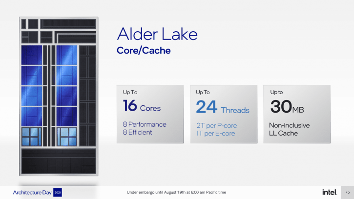
Alder Lake-S will include 8 Golden Cove cores and 8 Gracemont cores, according to Intel, who verified this during the company’s architecture day. It will be manufactured utilizing Intel’s Intel 7 technology, which was previously known as the Intel 10 nm Enhanced SuperFin process. As previously stated, Alder Lake-S will have 8 Golden Cove cores, which are high-performance cores, and 8 Gracemont cores, which are high-efficiency cores. Due to the fact that Gracemont cores do not support Hyper-Threading (HT), Alder Lake-S will only be able to provide 16 cores and 24 threads, which is the same as the presumed i9-12900K configuration.
CPU
Further information: Golden Cove (microarchitecture) and Gracemont (microarchitecture)
Golden Cove high-performance CPU cores
New instruction set extensions[6]
Gracemont high-efficiency CPU cores
Next-generation hardware scheduler; adding support for these advanced scheduling capabilities will require Microsoft to add support for them to x86-64 Windows.
GPU
Intel Xe (Gen12.2) GPU
I/O
New LGA 1700 socket[8]
PCI Express 5.0
DDR5 memory support for desktop CPUs
LPDDR5 memory support for laptop CPUs
DMI 4.0 x8 link with Intel 600 series PCH chipsets
Above you can see three markets differentiated versions of alder lake. For us, Guru’s the most left one is the most important. It is possible to view the eight high-performance cores (golden cove) in dark blue, as well as the energy-efficient Gracemont cores, which are visible below them in light blue. The integrated graphics is based on Xe, and it has up to 96 EUs for the GPU and 32 EUs for media functions only, according to the manufacturer.
For a fully equipped processor, you’ll receive eight performance cores as well as eight energy-efficient cores; the performance cores have SMT (hyper-threading), which means you’ll end up with a total of 24 CPU threads. In the following chapters, we’ll dive into greater depth about architecture.
The Memory subsystem and PCI_Express 5.0
The memory subsystem, which is DDR4 and DRR5 compatible, has a large amount of transistor real estate Intel clearly invested heavily in it.
Intel continues to list memory at the JEDEC specification level, implying that it is unable to go any further. DDR4 memory operates at 3200 MHz, while DDR5 memory operates at 4800 MHz by default. You can already see that the memory bandwidth is likely to rise dramatically with DDR5 technology.