ASUS Maximus Z690 Hero review Introduction
ASUS Maximus Z690 Hero review Introduction
To be precise, ASUS is back in the game, this time with another HERO, in the form of a Z690 motherboard. This Alder Lake motherboard is loaded with features and gadgets, and it’s dressed to impress with its dark design. The Z690 motherboards from ASUS will be plentiful, with some of the models offering a choice between DDR5 and DDR4 memory configurations. It all starts with the flagship ASUS ROG Maximus Z690 Extreme motherboard, which is followed by the FORMULA, HERO, and APEX motherboards, all of which will include DDR5 memory and only DDR5 memory — and that’s all there is to it. In total, there will be three ROG STRIX Z690 motherboards, one TUF GAMING Z690 motherboard, and a slew of PRIME Z690 motherboards, all of which will have differing degrees of technological sophistication, features, and sizes. ProART Z690-Creation 10G motherboard, which sounds like it’ll be a “content creator” motherboard with 10GbE LAN connectivity and, I’m sure, a ton of I/O connectivity, will be sandwiched between the rest of the ASUS Z690 lineup. The ASUS Maximus Z690 Hero, as tested today, rocks a 20-phase power design with 90A PowerStages.
Alder Lake and Z690
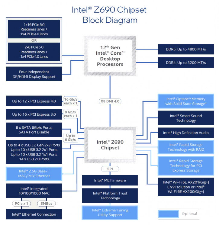
DDR5 and PCIe Express 5.0 are among the first-ever for intel products. Z690 is the enthusiast chipset from Intel, and this motherboard is powered by it. It also marks the dawn of a new era, Alder lake processors are a completely new and faster architecture from Intel. We have written a lot about it, bus basically the new processors will have energy and performance cores to balance power consumption in idle and load conditions. next to that with the Alder lake platform new features are brought to the table.
BIG versus little
As an alternative to Intel’s previous releases, which focused solely on single-core and gaming performance, Alder Lake puts the company fully back in the multi-core ring, led by its squad of sixteen-core goliaths built on Intel’s transistor-dense 10-nanometer manufacturing process. But this time, Intel delivers its own interpretation of the term BIG.little. We’ll talk a little more about it on the next pages.
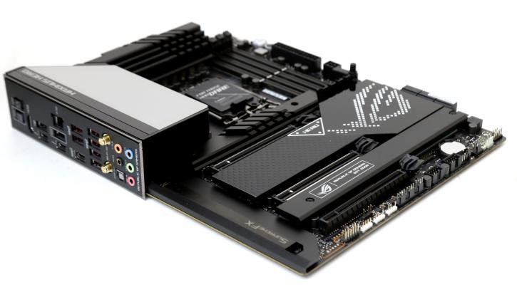
ASUS Maximus Z690 Hero
Starting with the basics, the Maximus Z690 Hero is more than capable of handling the most powerful CPUs that Intel has to offer this generation, including the Core i7 and i9 processors. The new p- and e-core design places more demands on the operating system to delegate duties in a more dynamic manner, necessitating the development of a motherboard power supply circuit that can react quickly to changes in load. In order to achieve this requirement, the Hero is equipped with a battery of twenty 90A power stages, which are organized into ten paired phases, which ensures that transitions between efficiency and performance cores are handled as seamlessly as possible.
Adoption of PCIe 5.0 may take some time, DDR5 memory is however is here, and for the most majority of users, it will have a greater impact on their day-to-day computing speed. While the shift in memory architecture has presented issues, one of the most significant modifications from DDR4 to DDR5 has been the insertion of a PMIC, or power management integrated circuit, on the memory module itself. The PMIC introduces a voltage lock on some lower-end memory modules that are coming out this generation, limiting the amount of potential performance that can be extracted from the kits. Engineers of this mobo have discovered a means to unlock those PMICs, allowing extra power to be delivered to the DIMMs, allowing for faster frequency response and tighter timings. Even with kits that weren’t built for overclocking, enthusiasts can locate options in the UEFI that allow them to manually alter the PMIC voltage and perform some basic overclocking. But let’s startup the review.
Alder Lake – a Hybrid Computing Architecture
It hasn’t exactly been a secret that Intel has been putting in significant effort to re-take the CPU market. After numerous respins, it was time for a new architecture, created from the ground up with a hybrid design; meet Alder Lake, which you’ve probably already heard a lot about. They will also be the first to adopt a hybrid architecture, similar to ARM’s BIG.little, that combines high-performance cores combined with efficient ones, making them the first of their kind for Intel. Furthermore, this new generation is now proven to be the first to support DDR5 memory (DDR4 compatible memory controllers as well) and PCI-Express 5.0, making it the first generation to do so.
Alder Lake CPU architecture has two different CPU cores
The following are a set of slides from the presentation that you can view. As previously indicated, we acquired this information hours before the embargo was lifted and will fill in the gaps throughout the day. Mind you the Core i9-12900K has 16 cores and 24 threads. 8 P-Core (16 threads) and 8 E-Core (with 8 threads). The CPU has 30 MB L3 cache, 3 MB per core (Golden Cove) and 3 MB per cluster (E-Core) (Gracemont). That’s 8 P-Cores for 24 MB and 6 MB from each of the two clusters of 4 E-Cores. The chip has 12.5 MB of L2 cache and 1.25 MB of L3 cache.
Gracemont (energy efficient cores)
Alder Lake is Intel’s codename for the 12th-generation of Intel Core processors based on a hybrid architecture utilizing Golden Cove high-performance cores and Gracemont power-efficient cores. According to Intel, Alder Lake is a “performance hybrid” in their portfolio, as it is focused on performance rather than power consumption. Gracement, wasn’t that Intel Atom related? Gracemont is an upcoming microarchitecture for low-power processors that will also be used in Intel’s systems on a chip (SoCs). It will be the successor of the Tremont microarchitecture. Additionally, it will be deployed as low-power cores in a hybrid architecture for Intel’s Alder Lake processors, similar to its predecessor. The cores have been further enhanced. Gracemont is actually the 4th generation out-of-order low-power Atom microarchitecture, built on the Intel 7 manufacturing process. Intel also says that Alder Lake will provide the most performance per watt of any of its processors. You’re going to notice a number of things, among them, increases in L1 caches; the Instructions cache for example was doubled to 64KB with an up to 4MB L2 cache, remember we’re still talking the energy-friendly cores here. Microsoft will have to introduce support for these sophisticated scheduling features to x86-64 Windows in order for them to be supported for the next-generation hardware schedulers. Key changes:
64KB per core Level 1 instruction cache
DDR5 memory
PCIe 5.0 support
Support for AVX, AVX2, and AVX-VNNI instructions
The Hybrid Architecture in Alder Lake is much different from that of hybrid concepts such as those we are familiar with in smartphones, such as Arm’s BIG.little processor. The most important goal of various smartphone technologies in the smartphone world is to save on energy consumption. This is undeniably one of the benefits of Intel’s Hybrid Architecture, but the increased efficiency will also result in a higher overall perf level as a result of increased efficiency.
Golden Cove (performance cores)
The architecture diagrams of the low-power Gracemont cores have just been presented to you, however, Alder Lake will make use of its Golden Cove CPU cores when speed and performance is critical. And these should make a significant difference in IPC when it comes to processing data compared to say Comet- and Rocket lake. Golden Cove CPU microarchitecture will take the place of the Sunny Cove, Willow Cove, and Cypress Cove microarchitectures, according to Intel. Originally described to as 10 nm Enhanced SuperFin, it will be made using Intel’s Intel 7 manufacturing node, which was introduced in 2012. (10ESF). These high-performance cores will find their way into scalable processors such as Alder Lake and Xeon, as well as Sapphire Rapids. According to Intel, all of the enhancements combined should result in an improvement in IPC of 19 percent, which is on par with or slightly higher than the improvement achieved by Sunny Cove when compared to Skylake. That should even be sufficient to dethrone the Zen 3 architecture of the Ryzen 5000 CPUs.